Single-Photon Avalanche Diode Micro-Arrays Directly,
Epitaxially Integrated on Silicon Substrates for Photon-Number,
Resolution and Quantum Information Applications.

Heteroepitaxy of Sb-based III–V SPADs on Silicon

Why Sb-based SPADs on Si?
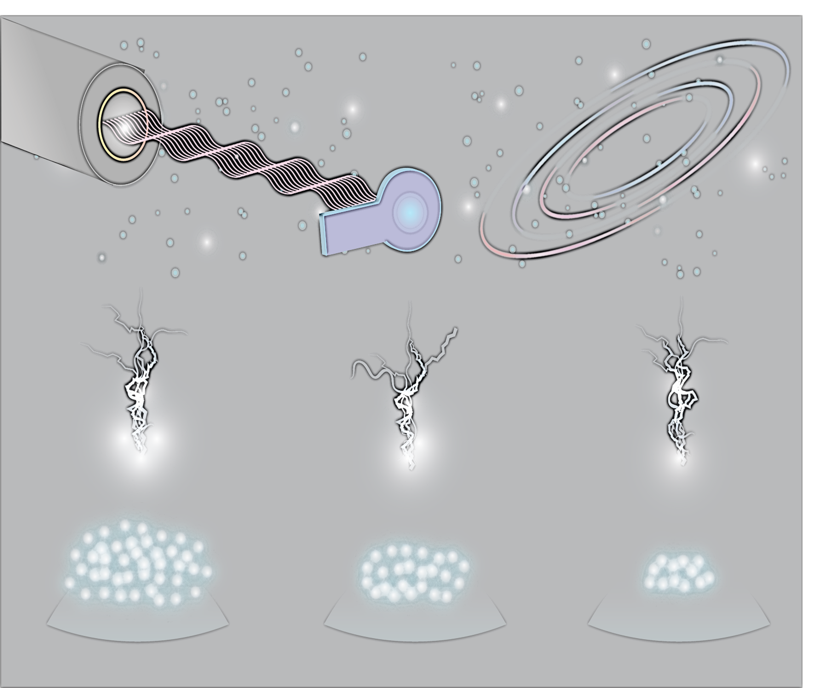
  • SPADs enable single-photon detection for LiDAR, quantum communication, and biomedical imaging.
  • Silicon SPADs are limited to the visible range. Performance drops sharply beyond ~1 μm.
  • Sb-based III–V materials (InGaAsSb, AlGaAsSb) cover the SWIR range (1.3–2.5 μm) with:
    • Tunable bandgap
    • Lower Auger recombination
    • Lower excess noise compared to InGaAs/InP
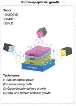
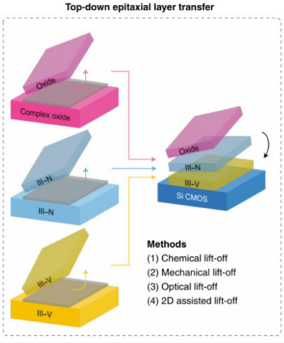
  • Integrating Sb-based SPADs on silicon enables SWIR detection + CMOS scalability.
Bottom-up epitaxial growth
Top-down epitaxial layer transfer
Why This Topic Matters Now
  • Strong demand for low-cost, large-format SWIR SPAD arrays.
  • InP substrates are expensive and limit integration density.
  • Sb-based III–V-on-Si aligns with:
    • Heterogeneous integration
    • Silicon photonics
    • On-chip detector–readout co-integration
  • Recent progress in buffer layers and defect reduction shows feasibility.

SPAD as SPD and PNRD (Device vs. System Level)

Device level (Single photon detector):

A single SPAD operated in Geiger mode produces a binary avalanche from one photon → single-photon sensitivity.

System level (Photon number resolving detector):

Photon-number resolution is achieved by spatial multiplexing, temporal multiplexing, or modulating in, mapping multiple avalanches to photon number.

Device vs System Level Response
SPD
SPD Circuit
PNRD (temporal multiplexing)
PNRD Temporal Multiplexing 1 PNRD Temporal Multiplexing 2
PNRD (Spatial multiplexing)
PNRD Spatial Multiplexing Device
PNRD Spatial Multiplexing Graph

Inherent capability by gain regulation

Using an ultra-short quenching time under self-differencing mode or low-pass filter scheme, SPAD can also inherently exhibit PNR capability.

Inherent capability schematic

■ Poisson distribution: P(μ,n) = μne−μn!

P(V) = n=0 p(μ,n) · ρ(n,V)

Princeton lightwave SPAD graph
Self-fabricated SPAD graph

Direct MBE epitaxy of Sb material on Si substrate at NYCU

Layer Structure

Layer Structure

XRD Spectrum

XRD Spectrum

RSM

RSM
Theoretical value
Al0.3Ga0.7Sb = 60.592° = 6.10778 Å
GaSb = 60.723° = 6.0959 Å
AlSb = 60.290° = 6.135 Å
AFM Morphology

These results demonstrate that high-quality, uniform GaSb heterostructures were successfully heteroepitaxially grown on Si, evidenced by well-defined layer engineering, sharp XRD peaks with minimal center–edge variation, and smooth surface morphology.