
Observing the trends of system-level design, our research activities have been focusing on two major themes: (1) the electronic system-level design platform for many cores, and (2) test and diagnosis with machine learning techniques. The following is a detailed description of our research direction and results:
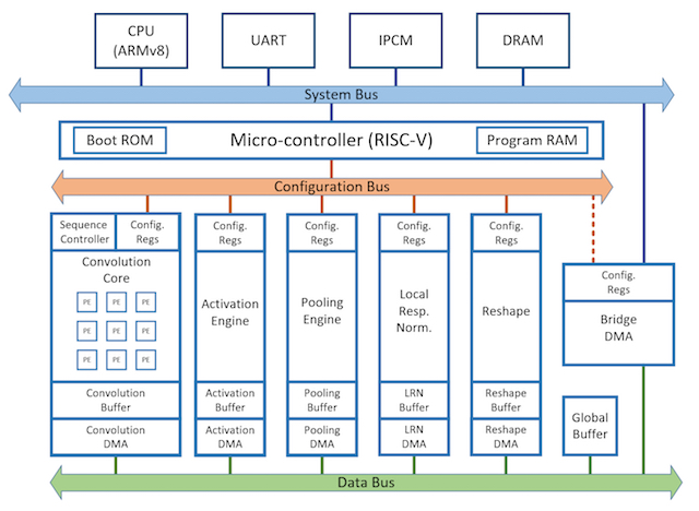
Design Platform for DNN Accelerators
Artificial Intelligence is current a hot topic among academic and industry research. To handle the complexity of learning algorithm and large amount of training/inference data, multitude of efforts are pursing acceleration architectures including NYU Neuflow, Movidius (Intel) Myriad, CAS DaDianNau and ShiDianNau, MIT Eyeriss, Google TPU, NVidia NVDla, etc. These examples highlight the fast progress aiming to develop a high efficient computing architecture. Yet, there are many technical challenges. Among them, we need to start from DNN framework (for training) such as Tensorflow, Caffe or Mxnet. To analyze the performance bottleneck of DNN networks, we can partition or prioritize hardware and software parts. And for the hardware accelerators, proper tuning of training process is also important (pruning, compression, quantization, etc.). We are collaborating with ICL/ITRI in developing high efficient DNN accelerator architectures.
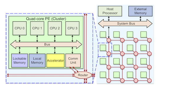
ESL platform for many-core systems
We have been developing an ESL design platform for many cores which includes processing elements (clusters of CPU cores with local memories), network-on-chip (NoC), and multi-channel external memories. Several parallel benchmark programs have been ported: object tracking, jpeg encoding, 3D pipeline rasterization, etc. The important features of this platform are:
- Standards compliant (SystemC, TLM and OCP)
- Efficient system libraries (message passing interface and pthread)
- All components have RTL synthesizable models (for accurate timing and power models)
- Processor-agnostic (been developed for RISC-V, MIPS, and OpenRisc)
- Integrate with DRAMSim2 for accurate DRAM timing models
For this platform, we have developed several techniques to improve the simulation speed and architecture performance:
Fast NoC timing simulator
Traditionally, a cycle-based model has to be implemented to obtain accurate simulation results for a worm-hole switching NoC, which could be complex and slow. We proposed and implemented an efficient and accurate timing simulator for NoC switching networks, which handles inter-packet traffic, FIFO management, flow control and different arbitration policies, etc. The simulator abstract on the timing behavior of a NoC with the same accuracy as a commercial RTL NoC circuits. The simulator can gain 73-95 times faster than a typical cycle-accurate SystemC model.
High-performance NoC network interface
The end-to-end data throughput at software layer on a NoC platform often cannot match the hardware native speed. We designed a high-throughput PE-to-PE communication unit with a corresponding driver layer on NoC-based many-core architectures. The proposed design can handle complicated message passing communications efficiently with application level flow control. The maximum throughput of a unidirectional transmission is 2687.3 Mbps, where the native NoC bandwidth is 3200 Mbps. As a comparison, a software-based protocol is only rated at 148.5 Mbps. The communication unit is also area-efficient of 19K gates, which is less than 3% of a single in-order RISC-based PE.
High-performance DRAM Simulator
We use transaction speculation to develop an event-based DRAM simulation model. By processing several memory commands at once, we can increase the simulation speed by 146.5 times without losing cycle accuracy.
System-level tracer for message passing APIs
We propose a debug tracer to record and convert information of high-level message passing APIs in hardware. The scheme can help designers to quickly understand the operation flow of a message passing system. We have used the tracers in a many core ESL platform to find out several bugs including a FIFO overrun, a fairness issue of a NoC switch, and a performance issue of a client-server parallel software. Since we record the trace data at API layer, we have a compression ratio of 99.77% when compared to signal level traces. For a 16-core system, the area overhead is only 40K gates which is equal to 1.5% of the complete platform.
Accelerator of Farneback Optical Flow
Farneback Optical Flow can estimate the displacement of a pixel at two time frames. It can capture the precise object tracking and predict movements. However, the complexity of the algorithm is usually very high. We apply a high-level synthesis flow to develop several parallelization and pipeline micro-architectures and memory management for the algorithm. And the final design can be implemented on a Xilinx Zynq FPGA board. The latency has been improved from 50ms to 6ms also with a reduction of memory bandwidth requirements.
Safety System Design
With the progress of autonomous car and production design automation, functional safety and system reliability has become increasingly important. For example, a SoC for auto system has to consider the full system effects. When a failure happens, the SoC and the system can safely detect and mitigate the effects without affecting passenger's life.
To analyze safety and reliability, we rely on functional fault simulation. Generally, a fault free simulation and an injected fault simulation are considered and compared at all registers/memories. However, as chip size grows larger, such approach faces several challenges: large circuit model (slow gate/RTL simulation), large faulty location/cycles, millions to billions of simulation cycles, etc.
In this project, we work with ICL/ITRL to use ESL approaches to develop design and analysis flows for functional safety and reliability.
Test and diagnosis with machine learning techniques
The objective is to develop methods and flows for efficient test and diagnosis on systematic process variations and to use the results to further tune on-chip hardware parameters to increase product yield.
Post-silicon variability measurements
The proposed method outputs most probable gate/interconnect delays that matches the measured path delays under the nominal delay distribution. Unlike the previous diagnosis methods, our method does not take any assumption on defect numbers, sizes and types (models), and thus it can be used to diagnose performance bottlenecks resulted from systematic variations. The experimental results show that the average correlation achieves 0.848 between estimated (by the proposed method) and sampled segment delays (generated from process models) for ISCAS89 benchmarks.
Diagnosis-assisted supply voltage configuration to Increase yield
A diagnosis technique based on delay testing has been developed to map the severity of process variation on each cell/interconnect delay. Given this information, we demonstrate a post-silicon tuning method on row voltage supplies (inside a chip) to restore the performance of failed chips. The method uses the performance map to set voltages by either pumping up the voltage on cells with worse delays or tuning down on fast cells to save power. On our test cases, we can correct up to 75% of failed chips to pass performance tests, while maintaining less than 10% increase over nominal power consumption.
SVM classification of multiple-clock test data
We propose to build a test data library that only uses a few fixed test clocks. We can then use the library to categorize the test results and sort the chips into different correction voltage tuning configurations. The experimental results show that with much lower cost (4% in average), the method can fix from 86% to 118% chip samples as compared to a satisfiability (SAT)-based method that requires accurate path delay measurement.
Post-silicon Aging Prediction
To test a circuit aging, we usually apply burn-in at a higher voltage or temperature. But this process is costly and may damage the product. We propose to predict the NBTI aging of a chip by signal stress level simulation and measurements of variability of transistor parameters. The results can be very close to the most accurate oracle (< 5% error rates).