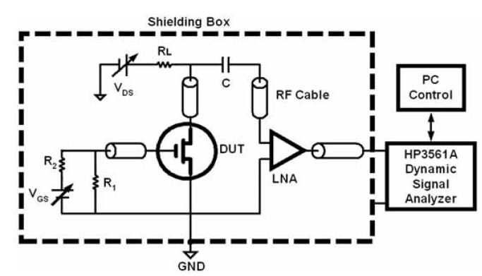
Flicker noise of devices is the main limitation to achieve a low phase noise voltage controlled oscillator (VCO). In many analog/digital and digital/analog converters, the flicker noise also degrades the signal to noise ratio. We have studied the flicker noise in various devices including CMOS transistors, GaAs MOSFETs, and GaN-based HEMTs. The figure below shows the flicker noise measurement setup in this study. Low-loss RF cables and probes with excellent ground shielding were used for the signal paths. In addition, the devices and the system including the preamplifier and the probe station were enclosed in a shielding box to further reduce the environmental interference. Moreover, a battery-powered DC voltage source was employed to prevent the additional noise introduced by the power supply.
- Flicker noise measurement setup
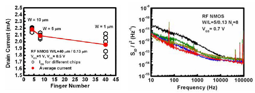
Studies of this topic were supported by the NSC project (93-2215-E-007-023-) about flicker noise characterization and modeling. The figures below shows the impact of shallow-trench-isolation (STI) effect on 0.13-μm RF NMOS transistors with different geometries for the DC current. The flicker noise spectrum density shows a wide variation of noise levels affected also by STI effect.
- Impact of STI effect on RF NMOS devices
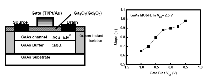
In addition, we have investigated the flicker noise characteristics in GaAs MOSFETs for the first time. With the improvement in Ga2O3(Gd2O3) insulators, the GaAs MOSFETs reveal the possibility for high-speed and high-power applications, resulting from an electronic mobility that is about five times greater than that in Si, and the advantage of semi-insulating substrate. The figures below show the device cross-section, and the slope g of the 1/fg characteristics as a function of gate bias. The measurement results indicate that the drain noise current density is comparable to that in modern CMOS technology. Studies on the bias dependence and the slope g suggest that the main noise origin located close to the Ga2O3(Gd2O3) insulator and channel interface.
- Flicker noise characteristics in GaAs MOSFETs
- C. Chan, Y. Lin, Y. Huang, S. Hsu, and Y. Juang, "Edge-extended design for improved flicker noise characteristics in 0.13-um RF NMOS," accepted for IEEE MTT-S Int. Microwave Symp. Hawaii, June 2007.
-
C. Chan, J. Jin, Y. Lin, S. Hsu, and Y. Juang, “STI Effect on Flicker Noise in 0.13-µm RF NMOS,” European Solid-state Device
Conference (ESSDERC ), pp.101-104, 2006.
-
C. Chan, P. Tsai, T. Lee, S. Hsu, J. Kwo, and M. Hong, “Flicker noise characteristics in GaAs MOSFETs,” MBE conference, September, 2006.
-
S. Hsu and D. Pavlidis, “A comparison of low-frequency noise characteristics and noise origins in InP-based NPN and PNP heterojunciton bipolar transistors,” IEEE Trans. Electron Devices, vol. 50, no. 9, pp. 1974-1982, Sep. 2003.
-
S. Hsu, D. Pavlidis, and D. Sawdai, “Low-frequency noise characteristics of PNP InAlAs/InGaAs HBTs,” IEEE Electron Device Letters, vol. 23, no. 12, pp. 688-690, Dec. 2002.
-
S. Hsu, D. Pavlidis, J. S. Moon, M. Micovic, D. Wong and T. Hussain, “Gate and drain low-frequency noise models of AlGaN/GaN
MODFETs,” proceeding of IEEE Lester Eastman conference, pp. 453-460, Aug., 2002.
Power characteristics and modeling
-
S. Hsu, B. Bayraktaroglu, and D. Pavlidis, “Comparison of conventional and Thermally-Stable Cascode (TSC) AlGaAs/GaAs HBTs for
microwave power applications,” Journal of Solid-State Electronics, vol. 43, no. 8, pp. 1429-1436, 1999.
-
S. Hsu, D. Pavlidis, “Analysis and modeling of dispersion characteristics in AlGaN/GaN MODFETs,” proceeding of 25th IEEE GaAs IC
Symposium, Nov. 2003, pp. 119-122.
-
S. Hsu, P. Valizadeh, D. Pavlidis, J. S. Moon, M. Micovic, D. Wong and T. Hussain, “Study on large-signal linearity and efficiency of
AlGaN/GaN MODFETs,” proceeding of 31st European microwave conference, 2002.
-
S. Hsu, D. Pavlidis, J. Moon, M. Micovic, C. Nguyen, and D. Grider, “Low noise AlGaN/GaN MODFETs with high breakdown and power characteristics,” 23rd IEEE GaAs IC Symposium, pp. 229-232, 2001.
-
J. A. Yeh, C. A. Chang, C. -C. Cheng, J. -Y. Huang, and S. Hsu, “Microwave characteristics of liquid crystal tunable capacitors,” IEEE Electron Device Lett., vol. 26, pp. 451-453, July 2005.
-
X. Zhu, S. Hsu and D. Pavlidis, “First microwave characteristics of InGaAlAs/GaAsSb/InP double HBTs,” Topical Workshop on
Heterostructure Microelectronics for Information Systems Applications, W-9, Okinawa, Japan, Jan. 21-24, 2003.