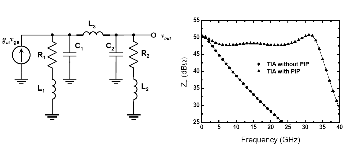
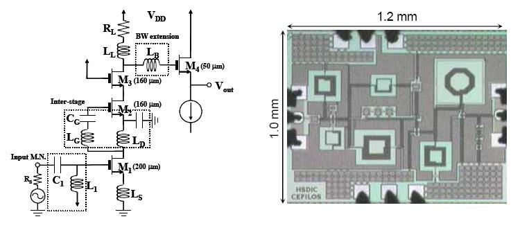
One of the main bottlenecks for achieving high-speed optical fiber communication is the solid-state circuits in the system, especially the front-end circuits. We focus on designing of 40-Gb/s transimpedance amplifier (TIA) at the receiver end in a standard CMOS technology, which was supported by NSC grant (92-2213-E-007-097-). A 40-Gb/s transimpedance amplifier (TIA) was realized in 0.18-µm CMOS technology and a transimpedance gain of 51.0 dBΩ and a 3-dB bandwidth up to 30.5 GHz were observed. A new bandwidth enhancement technique, π-type inductor peaking (PIP), is proposed, which gives a bandwidth enhancement factor of 3.31 without disturbing the low-frequency gain. The TIA presents the widest bandwidth and highest GBP/Pdc of 180.1 GHzΩ/mW among the published results with similar technologies. More details can be find in the listed papers.
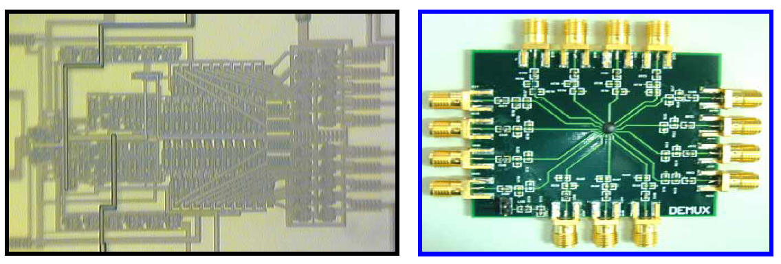
To expand our horizons in research, we also work together with the network switching design team leading by professor C. Chang (NTHU) under the NSC program 95-2752-E-007-002-PAE. The goal is to realize a high-speed scalable load-balanced Birkhoff-von Neumann TDM switch by IC process. We are in charge of the mixed-mode/RF portions of this design. The figures below show the chip photo of a 1:20 DEMUX and the customized PCB with SMA connectors for high-speed chip measurements. Our ultimate goal is to construct a 8´8 TDM switch on a single chip.
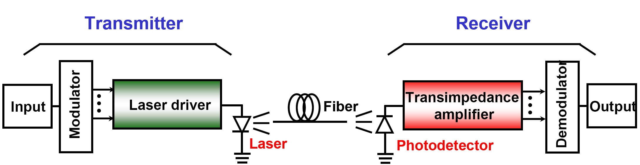
- A typical optical fiber communication system
- The proposed p-inductive peaking (PIP) technique for wideband circuits
- A high-speed 1:20 DeMUX in 0.18-mm CMOS technology for optical communication
-
J. Jin and S. Hsu, “40-Gb/s transimpedance amplifier in 0.18-µm CMOS technology,” European Solid-state Circuit Conference
(ESSCIRC), pp. 520-523, Sep. 2006.
-
X. Zhu, J. Wang, D. Pavlidis, and S. Hsu, “First demonstration of low-power monolithic transimpedance amplifier using InP/GaAsSb/InP DHBTs,” IEEE MTT-S Digest, pp. 101-103, June, 2005.
-
C. Hsiao, M. Kao, C. Jen, Y. Hsu, P. Yang, C. Chiu, J. Wu, S. Hsu and Y. Hsu, “3.2 Gbit/s CML transmitter with 20:1 multiplexer in 0.18-um CMOS technology, “IEEE Int. Conf. Mixed Design of Integrated Circuits and Systems, pp. 179-183, 2006.
-
C.-T. Chiu, J.-M. Wu, S. Hsu, M.-S. Kao, C.-H. Jen, and Y.-S. Hsu, “A 10Gb/s wide-band current-mode logic I/O interface for high-speed interconnect in 0.18-um CMOS technology," IEEE Int. SOC Conf., pp. 257-260, Sep. 2005.
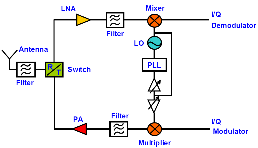
Circuits for wireless communications attract much attention from both industry and academia. We are particularly interested in the high-speed front-end circuit blocks including low-noise amplifiers (LNAs), voltage-controlled oscillators (VCOs), mixers, and power amplifiers (PA). A typical RF front-end configuration for wireless communication is shown below, which is probably the most challenging part in the overall system due to the high operation frequency. Knowledge of both analog and microwave circuits is required for designing high performance RF circuits.
- A typical RF front-end configuration in a wireless communication system
A 3.1-10.6 GHz ultra-wideband low noise amplifier utilizing a current-reused technique and a simple high-pass input matching network is shown in the figures below. The implemented LNA demonstrated a maximum power gain of 16 dB, and an excellent noise figure of 3.1 - 6 dB was obtained in the frequency range of 3.1-10.6 GHz with a power dissipation of 11.9 mW under a 1.8 V power supply. The proposed UWB LNA demonstrates the highest power gain and lowest noise figure among the published works in 0.18-μm CMOS technology.
- A 3.1-10.6 GHz ultra-wideband (UWB) low-noise amplifier (LNA) using current-reused technique
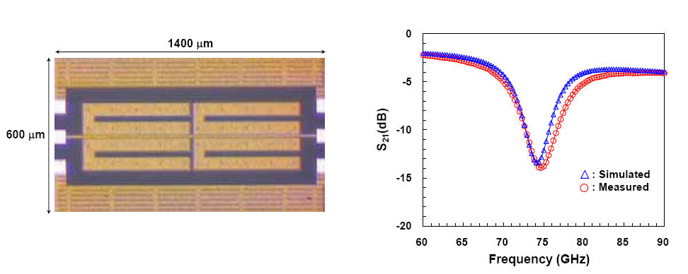
We have also explored the MMIC design up to W-band (75 GHz to 110 GHz) for resonator applications using standard CMOS technology. A high-Q multiple-ring resonator fabricated by standard 0.18-μm CMOS process was realized. This design achieves a high quality factor at W-band without the need of any post-processing steps. The measured quality factors are 38 and 83 at ~75 GHz under the loaded and unloaded conditions, respectively.
- W-band multiple-ring resonator by standard CMOS process
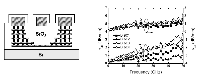
Interconnects play an important role in modern IC industry as the circuit operation speed entering the microwave frequency range. We proposed a novel semi-coaxial (SC) interconnect structures for both single-ended and differential type to reduce the signal loss and crosstalk. The single-ended semi-coaxial (S-SC) line shows the lowest loss of ~ 0.90 dB/mm at 50 GHz compared to other published results in standard CMOS technology and the differential semi-coaxial (D-SC) line also presents a very low differential-mode α of ~ 1.00 dB/mm at 50 GHz. The figures below are the cross section of a S-SC line and the differential-mode loss factor α (αdd) and common-mode α (αcc) for a D-SC line.
- Low-loss semi-coaxial interconnects in standard CMOS process
-
Y. Lin, S. Hsu, J. Jin, and C. Chan, “A 3.1–10.6 GHz ultra-wideband CMOS low noise amplifier with current-reused technique,” accepted for IEEE Microwave and Wireless Component Letter (to appear in March 2007).
-
X. Zhu, J. Wang, D. Pavlidis, and S. Hsu “InP/GaAsSb/InP DHBT technology and its application to MM-wave integrated oscillators,"
proceeding of 30th Workshop on Compound Semiconductor Devices and Integrated Circuits in Europe (WOCSDICE) 2006.
-
S. Hsu, H. Zhu, “W-band multiple-ring resonator by standard 0.18-um CMOS technology,” IEEE Microwave and Wireless Component
Lett., pp. 832-834, Dec. 2005.
-
J. Jin, S. Hsu, M. T. Yang, and S. Liu, “Low-loss differential semi-coaxial interconnects in CMOS process,” IEEE Trans. Microwave
Theory Tech., vol. 54, no. 12, pp. 4333-4340, Dec. 2006.
-
D. Cui, D. Pavlidis, S. Hsu, D. Sawdai, P. Chin, and T. Block, “First demonstration of monolithic InP-based HBT amplifier with PNP active load,” IEEE Electron Device Letters, vol. 23, no. 3, pp. 114-117, Mar. 2002.
- D. Cui, S. Hsu and D. Pavlidis, “Ka-band oscillators using InP-based HBTs,” Journal of Solid-State Electronics, vol. 46, no. 2, pp. 249-253, Feb. 2002.
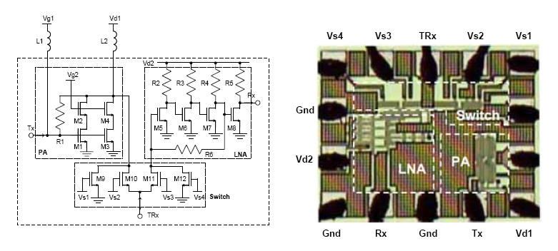
We also collaborated with professor L. Fan (NTHU) as a subproject under the contract “Nano-MRI Platform for Cell-Based High-Content, High-Throughput Screening” from NSC National Science and Technology Program for Nanoscience and Nanotechnology. Within a nano-MRI system, a RF front-end circuit consists of a low-noise amplifier (LNA), a power amplifier (PA), and a switch is essential for signal detecting. The figures below show the circuit schematic and the micrograph of the fabricated IC with bond wires in 0.18-μm CMOS technology. The LNA is designed with a cascaded common-source configuration to meet the design specifications of 20 dB gain and 2 dB noise figure at the operation frequencies with both input/output reflection coefficients below -20dB. The PA and LNA are designed with shunt-shunt feedback for a wideband characteristic to cover the frequencies of 77MHz, 125MHz, and 500MHz. This study together with MEMS miniaturized MRI chip enables a desk-top cellular MRI system with micron resolution.
- RF front-end circuit for a Nano-MRI system
-
L. Fan, W. Huang, C. Cheng, P. Chu, H. Hao, C. Hsieh, S. Hsu, A. Jin, K. Hsueh, C. Lee, J. Chang, E. Liu, A. Huang, C. Chien, A. Yeh J. Chen, W. Wu, and C. Lai, “Magnetic resonance microsystems for life science applications,” Proc. of Transducers 2005, pp.1998-2001, Seoul, Korea, June 2005.
-
L. Fan, S. Hsu, J. Jin, C. Hsieh, W. Lin, H. Hao, H. Cheng, K. Hsueh, C. Lee,“Miniaturization of magnetic resonance microsystem
components for 3D cell imaging,” IEEE Int. Solid-State Circuit Conf. (ISSCC), San Francisco, pp. 166-168, Feb. 2007.