Chap#3.
Boolean Algebra and Logic Design
@
Topic
-
Digital circuits are composed
of gates, and flip-flops.
-
Boolean algebra.
3.1
Algebraic Properties
-
Define
Math System by
1.
A set of element
2.
A set of operator
3.
A number of unproved Axiom
-
Define
ordinary algebra
by
1.
R ( infinite set of elements )
2.
{ +, -, *, / }
3.
Some Axiom ( P064
)
3.2
Axiomatic Definition of Boolean Algebra
-
In
1854, George Boole introduced Boolean Algebra
-
In
1938, C.E.Shannon applied
A two valued Boolean algebra (switching algebra)
to electrical switching circuit
-
In
1994, E.V.Huntington formulate Boolean algebra
-
Define
Boolean algebra
by
1.
B ( undefined set of elements )
2.
{ +, *, ' }
3.
Some Axiom ( P065
)
-
Define
Two Valued Boolean
algebra by
1.
B ( { 0, 1 } )
2.
{ +, *, ' }
3.
Some Axiom
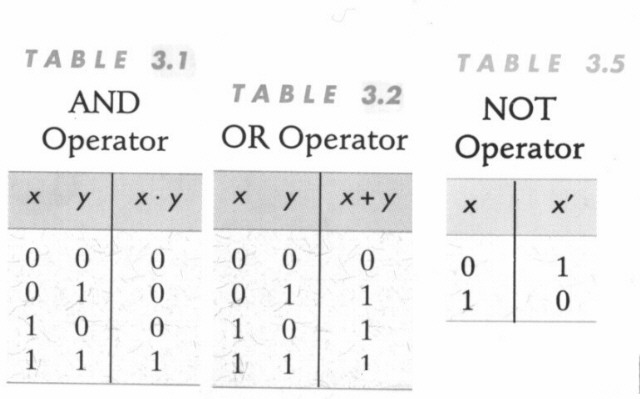
Axiom 1 : Closure ( P066
)
Axiom 2 : Identity element --- x*1=x; x+0=x
Axiom 3 : Commutative --- x+y=y+x; x*y=y*x
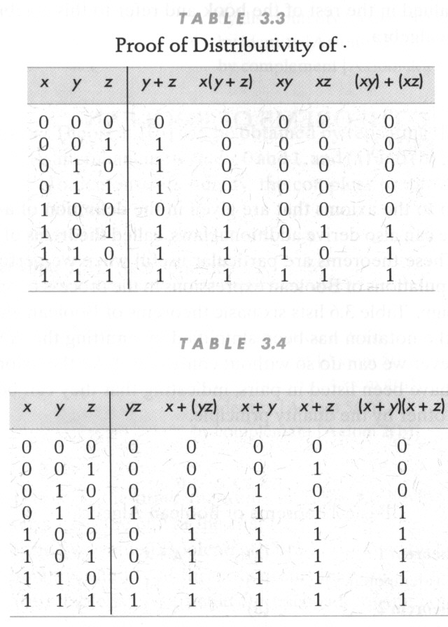
Axiom 4 : Distributive ( P067
)
Axiom 5 : Complement element ( P066
)
Axiom 6 : Cardinality --- has two distinct elements
1 and 0, and 1 != 0
3.3
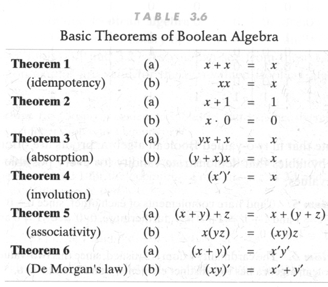
Basic Theorems of Boolean Algebra
-
Basic
Theorems of Boolean Algebra ( P068
)
-
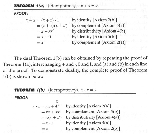
Theorem 1 : Idempotency
proof ( P069A )
-
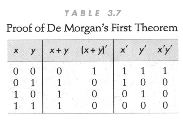
Theorem 6 : De Morgan's
laws proof ( P069B )
General form ( P070 )
3.4
Boolean Functions
-
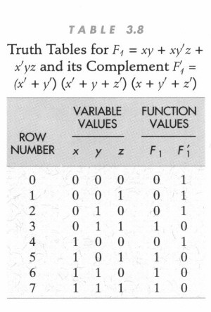
Boolean
Functions : F1 = xy + xy'z + x'yz
-
3.4.1 Complement
of a Function :
F1' = (xy + xy'z + x'yz)' = (x'+y')(x'+y+z')(x+y'+z')
Expression to T/Tab ( P071
)
Graphic of F1 & F1' ( P073A
)
-
3.4.2 Algebraic
Manipulation
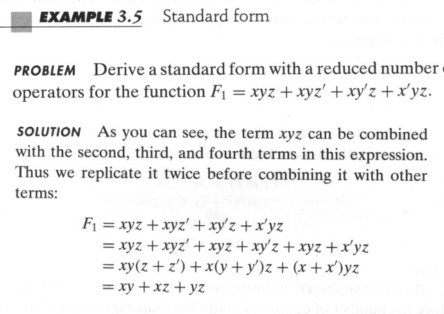
F1 = xy + xy'z + x'yz = xy + xz + yz
Reduce process ( P073B
)
3.5
Canonical Forms
-
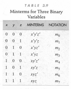
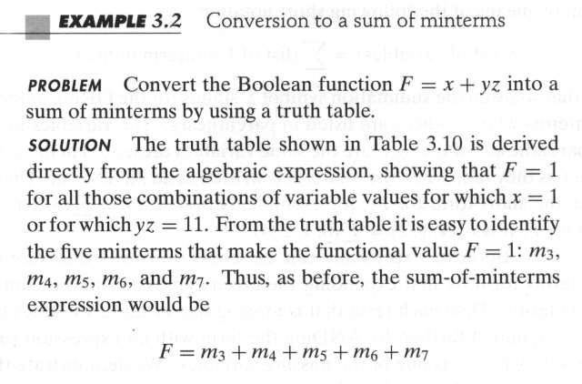
minterm
: AND term of n literals (
P075A )
-
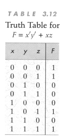
Any
Boolean function can be expressed as a sum of its 1-minterms
-
T/Tab for B/Func
( P075B )
-
F1 = sum of 1-minterms
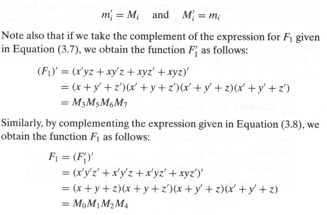
F1' = sum of
0-minterms
-
Sum-of-minterm expansion
( P075C )
-
Conversion to a Som
( P076A ) ( P076C)
-
---------------------------------------------
-
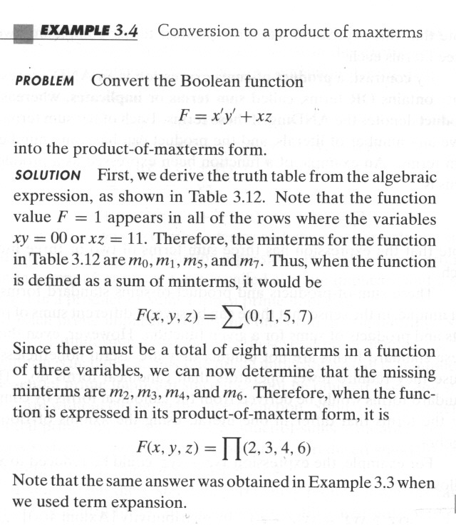
Maxterm
: OR term of n literals (
P076B)
-
Any
Boolean function can be expressed as a product of its 1-minterms
-
F1' = product of 1-Maxterm
( P077 )
F1 = product of
0-Maxterm
-
PoM expansion (
P078 )
-
PoM conversion (
P079B ) ( P079A )
3.6
Standard Forms
-
Two canonical form Som
and PoM provide unique
expressions
-
Two standard form
SoP : e.g. F1
= xy + xy'z + x'yz
PoS : e.g. F1' = (x'+y')(x'+y+z')(x+y'+z')
-
implicants = product terms
= AND terms
implicates = sum term
= OR term
-
e.g. Derive standard form
( P080 )
-
prime implicant : product
term of SoP
-
prime implicate : sum
term of PoS
-
essential prime implicant
:
1-minterm is included
in only one prime implicant
-
e.g. nonstandard forms
( P081 )
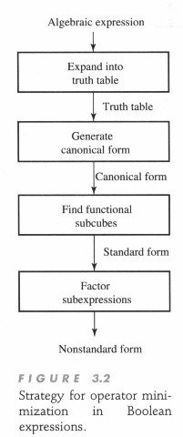
-
Strategy for operator
minimization ( P082 )
3.7
Other logic operations
-
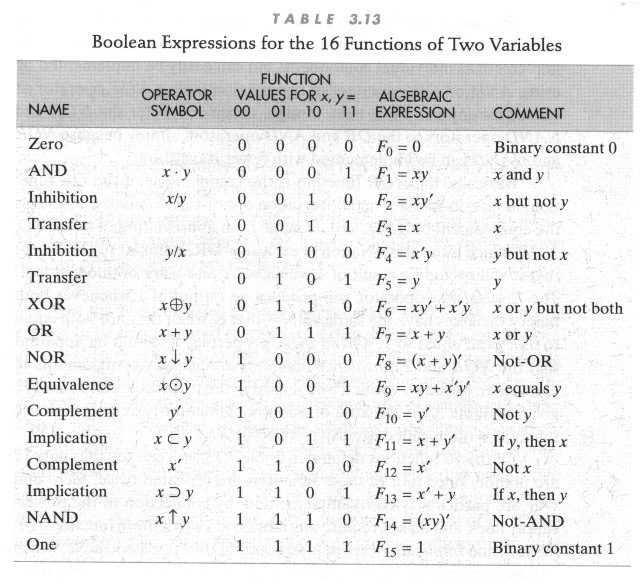
16
function of two variable ( P083
)
-
Three
categories :
1) 2 function
: Zero, One
2) 4 function
: complement and transfer
3) 10 function
:
-
NAND, NOR implemented
with fewer transistors
3.8
Digital Logic Gates
-
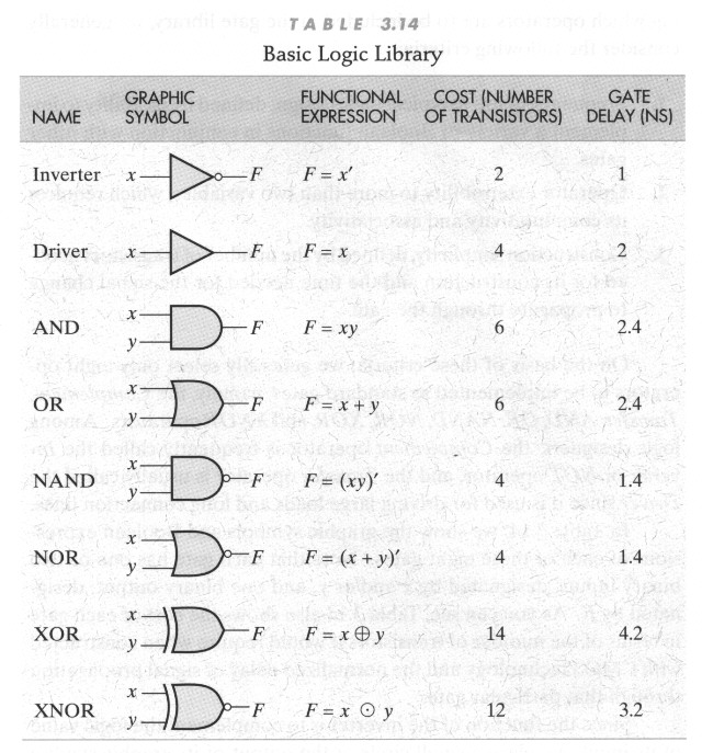
Gate Library : collection
of logic gates
-
standard gates : gates
in library
-
Criteria for operator
included in library
1) Frequency
of use
2) Operator
extensibility (require commutative and associative)
3) Construction
simplicity (lower cost and smaller delays)
-
Basic Logic Library
( P086 )
-
e.g. Full-adder design
1) True Table
( P087B)
2) Derive function
( P087A )
( P089
)
3) Implement
with AND, OR, XOR ( P088A
)
4) Implement
with NAND, NOR ( P088B
)
3.9
Extension To Multiple Inputs And Multiple Operators
-
AND & OR are commutative
& associative, so easy to extend
-
NAND & NOR are commutative,
but not associative
define : NAND(x,y,z,---)
= (xyz---)'
NOR(x,y,z,---) = (x+y+z+---)'
-
XOR & XNOR are both
commutative & associative
-
Multiple-input
standard logic gates ( P091
)
-
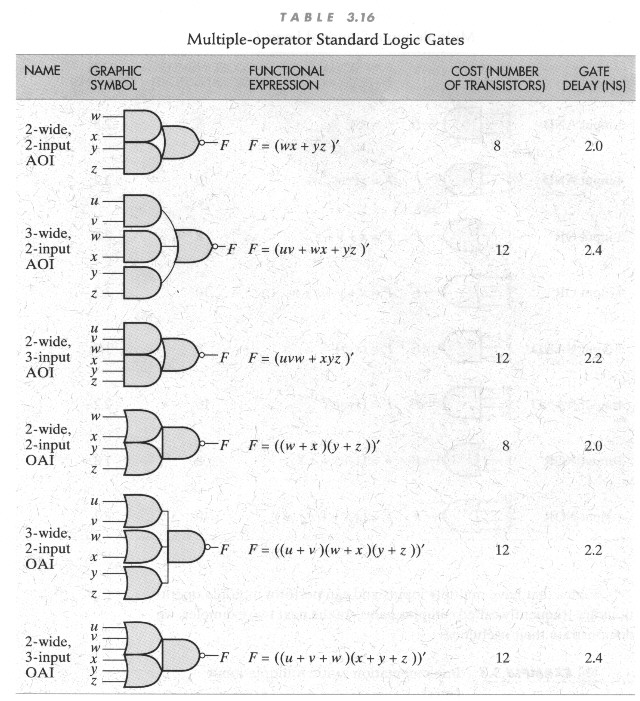
Multiple-operator
standard logic gates ( P092
)
-
e.g. F = (uvw + xyz)'
Imp with 2-3-AOI : Required 12
Q; 2.2 ns
Imp with two 3-AND and one 2-OR : Required 20 Q; 4.2 ns
-
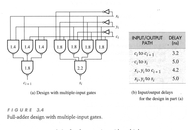
Imp with multiple-input
gates ( P093 )
-
Imp with multiple-operator
gates ( P094 )
3.10
Gate Implementations
3.10.1
Logic Levels
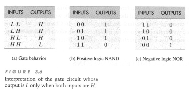
-
Positive logic system
: 0 -- L , 1 -- H
-
Negative logic system
: 0 -- H , 1 -- L
-
Interpretation (1)
( P096A )
-
Interpretation (2)
( P096B )
-
Logic Symbols (
P096C )
3.10.2
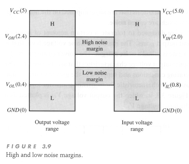
Noise Margins
-
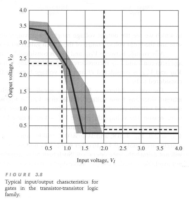
Noise margin : maximum
noise voltage
-
I/O characteristics
( P097 )
-
High and Low noise margin
( P098 )
-
High-Level noise margin
= VOH - VIH
-
Low-Level noise margin
= VIL - VOL
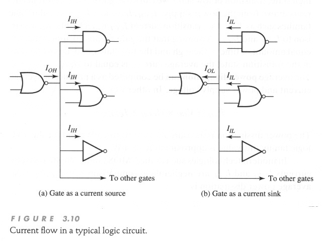
3.10.3
Fan-out
-
Fan-out : Standard load
( P099 )
-
Fan-out = max(IOH/
IIN , IOL/IIL)
3.10.4
Power Dissipation
-
TTL : PAVG
= VCC * (ICCH
+ ICCL)/2
-
CMOS : PAVG
= VCC * ICCT
3.10.5
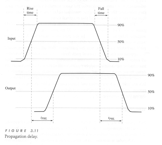
Propagation Delay
-
Propagation
delay (
P101 )
-
rise time : a signal to
switch from 10% to 90%
-
fall time : a signal to
switch from 90% to 10%
-
Propagation
delay tP = ( tPHL
+ tPLH ) / 2
3.10.6
Bipolar Logic Families
-
Transistor
technologies
1)
Bipolar transister model (
P103A )
(current control switch)
2)
MOS : Metal-Oxide-Semiconductor
-
1960
: RTL : Resistor-Transistor-Logic
-
19xx
: DTL : Diode-Transistor-Logic
-
1970
: TTL : Transistor-Transistor-Logic
-
TTL
gate Implementation ( P103B
)
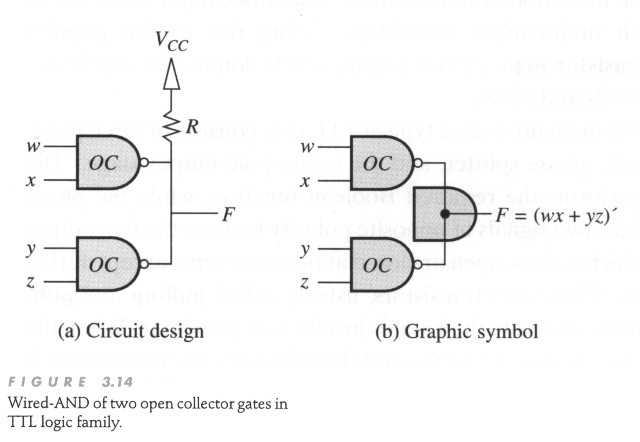
-
Wired-AND/AOI
Gate ( P104
)
-
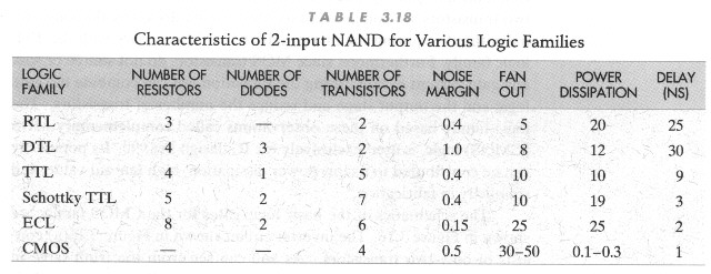
Characteristics
of 2-input NAND ( P105
)
3.10.7
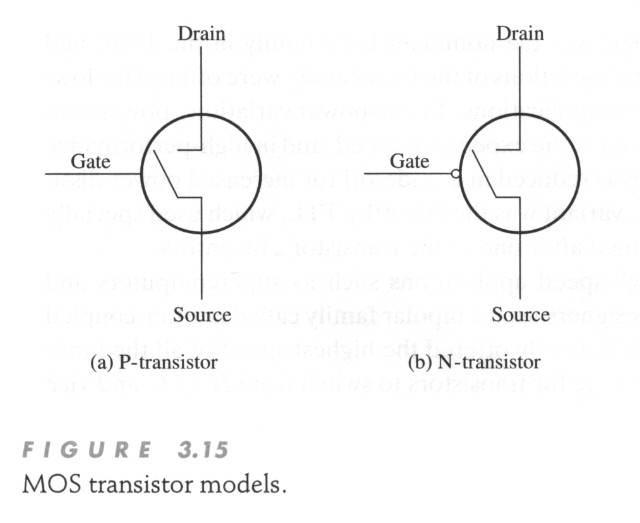
MOS Logic Families
-
MOS
transistor model ( P106
)
(Voltage control
switch)
-
1980
: MOS competitor to TTL
-
1990
: CMOS : complementary MOS
(N-Transistor
pull-up; P-Trasistor pull-down)
-
Basic
gate in CMOS tech. ( P107
)
3.11
VLSI Technology
-
IC : integrated circuit
( P109 )
-
SSI : Small-Scale-Integration
(gate < 10 ) ( P110 )
-
MSI : Medium-Scale-Integration
(10 < gate < 100 ) ( P111
)
-
LSI : Large-Scale-Integration
(100 < gate < 1000 )
-
VLSI : Medium-Scale-Integration
(gate < 10000 )
-
ASIC : Application-Specific
IC
-
VLSI
Design Approach
1)
Full Custom design
using standard cell | P086 |
P091 | P092
|
standard cell approach ( P112
)
Full adder implement with standard cell ( P113
)
2)
Semicustom design
using prefabricated gate array
(usually 3- or 4-input NAND or NOR)
e.g. Full adder implementation with gate array ( P114
)
3)
Field Programmable design
a) FPGA
approach are ideal for prototyping.
b) offer
a cost-effective solution for small-volume production
c) lower
density & speed
d) FPGA
( P115 )
e) Full
adder implement with one PLB ( P116
)
3.12
Chapter Summary
-
Boolean
Expression :
1)
Canonical form ( unique )
2)
Standard form
3)
Nonstandard form
-
VLSI
technology
1)
Full Custom technology
2)
Semicustom technology
3)
Field Programmable technology
-
Highest
performance
1)
minimal delay ( Time )
2)
minimal cost ( space )
3.13
Further Readings
-
(
P118 )
-
Quote
:
*
Minterm & Maxterm ( M044
)
*
Digital Gate ( M066 )
*
Switch Models for CMOS ( M084
)
*
Switch Models Network ( M085
)
*
CMOS circuit ( M086 )
3.14
Problems
-
3.1
(e), 3.4 (a), 3.5 (a), 3.7 (b),
-
3.14
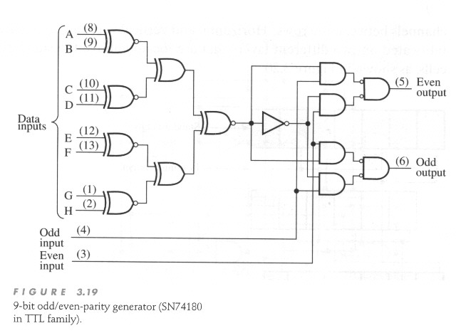
(a)(b)(c), 3.15 (a)(b)(c), 3.19 (a)